Difference between revisions of "8-Band Decoder"
| Line 21: | Line 21: | ||
===Wiring=== | ===Wiring=== | ||
| − | There are 3 logic input lines that run from the GPIO breakout board to J1: The LSB and the MSB come from the 4 band switch connector. The “T” (transverter) line comes from GPIO Pin 7 which you will find labelled as | + | There are 3 logic input lines that run from the GPIO breakout board to J1: The LSB and the MSB come from the 4 band switch connector. The “T” (transverter) line comes from GPIO Pin 7 which you will find labelled as "Pin 7" of the Digithin connector of the GPIO breakout board. These 3 logic lines also need to be routed to the 8-way RF switch. The current consumption of the board is low, so it could be powered by 3v3 from the Raspberry Pi. |
| − | You will also need to run wires from J2 to the VCO LO filter, as these should no longer be directly controlled by the RPi. | + | You will also need to run two wires from J2 of the 8-Band Decoder board to J3 on the VCO LO filter board, as these should no longer be directly controlled by the RPi. |
The PTT Jumper determines whether the Band Outputs are only active on transmit, or are active all the time. | The PTT Jumper determines whether the Band Outputs are only active on transmit, or are active all the time. | ||
Revision as of 12:03, 18 March 2018
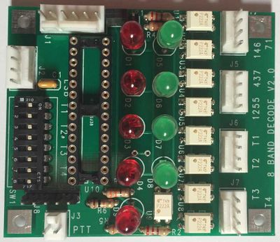
This 8-band decoder is designed to work with the 8-band RF output switch and the "Portsdown 2018" software. It will provide switching signals (either always on, or PTT activated) to 4 power amplifiers and 4 transverters, and it also enables you to set which VCO filter should be switched in for the 4 transverter outputs. PCBs will be available from the BATC Shop.
The firmware for the 16F883 PIC is available here: https://github.com/BritishAmateurTelevisionClub/8-Band-Decode.
The schematic is here:Media:8 BAND DECODE V2-0 SCH.pdf
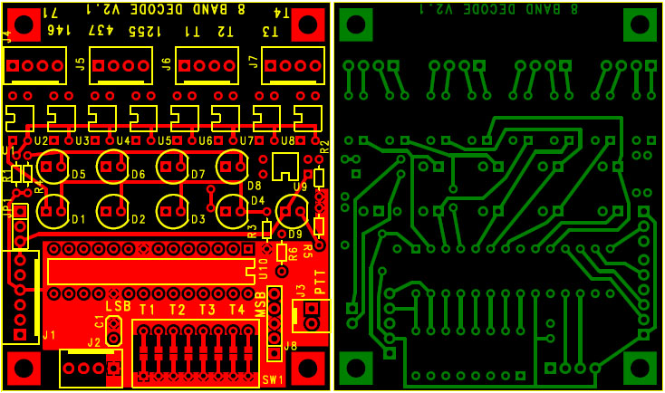
The board layout is here:Media:8 BAND DECODE V2-0 SS.pdf
The parts list, which is currently provisional, and only checked against the DigiKey Part Numbers, is here: File:8 BAND DECODE PARTS.xls
A drill template for the board (which has been designed to be a form and fit replacement for the 4-band decoder) is here: Media:8 BAND DECODE V2-0 DRILL TEMPLATE.pdf
PIC Programming
If you have a PIC programmer, you can program the 16F883 using the .hex file here https://github.com/BritishAmateurTelevisionClub/8-Band-Decode. If you program the PIC on the assembled PCB using the 5-pin ICSP header, make sure that the switches for T4 are in the off position as these pins are shared with the programming pins. The PIC will need to be powered with 5 volts for programming, either through the board supply or from your programmer. Note that in normal operation the board will be powered with 3.3 volts and application of 5 volts to program the PIC may damage other circuitry in your Portsdown if you do not disconnect the supply lead.
Alternatively, programmed PICs may be available from the BATC Shop.
Wiring
There are 3 logic input lines that run from the GPIO breakout board to J1: The LSB and the MSB come from the 4 band switch connector. The “T” (transverter) line comes from GPIO Pin 7 which you will find labelled as "Pin 7" of the Digithin connector of the GPIO breakout board. These 3 logic lines also need to be routed to the 8-way RF switch. The current consumption of the board is low, so it could be powered by 3v3 from the Raspberry Pi.
You will also need to run two wires from J2 of the 8-Band Decoder board to J3 on the VCO LO filter board, as these should no longer be directly controlled by the RPi.
The PTT Jumper determines whether the Band Outputs are only active on transmit, or are active all the time.
Setting the VCO Filter for Transverter Bands
One of the resons for using a PIC on this PCB is to allow the LO Filter to be set correctly for the Transverter bands. The 8 DIP switches (or solder bridges if the switch is not fitted) need programming depending on the IF frequency used for each transverter.
The board is marked with T1, T2, T3 and T4 to designate the pair of switches for each transverter; it is also marked with LSB (nearest J2) and MSB (nearest J3) Use the following table to determine the settings for each transverter.
| IF Frequency MHz | IF Band | LSB | MSB |
|---|---|---|---|
| < 100 MHz | 71 MHz | On | On |
| 100 - 250 MHz | 146 MHz | Off | On |
| 250 - 950 MHz | 437 MHz | On | Off |
| 950 - 4400 MHz | 23cms | Off | Off |
"On" is equivalent to bridged with solder.
Board Layout
The board layout for V2.1 (which is electrically the same as V2.0, but has some slightly larger holes for JP1 and J8 and 3mm mounting holes, is shown below.

