Difference between revisions of "Filter Modulator Version 1A Modifications"
| (9 intermediate revisions by 2 users not shown) | |||
| Line 1: | Line 1: | ||
| − | The following modifications improve the transmitted spectrum of the Version 1 PCBs, and bring them to Version 1A standard: | + | ===Board information - version 1=== |
| + | |||
| + | PCBs supplied before 28 February 2017 are Version 1 and the parts list and schematics are available for download: | ||
| + | |||
| + | *[[:File:Portsdown parts V1.xls| xls parts list file - not including V1a Components, so do not use]] | ||
| + | |||
| + | *[[:File:Portsdown parts V1A.xls| xls parts list file - with V1a Components and changes]] | ||
| + | |||
| + | *[[Media:RBTVMOD_30_SS_TOP.pdf|Board top layout]] | ||
| + | |||
| + | *[[:Media:RBTVMOD 30 SS BOT.pdf|Board bottom layout]] | ||
| + | |||
| + | *[[:Media:RBTVMOD 30 BLOCK.pdf| Block diagram]] | ||
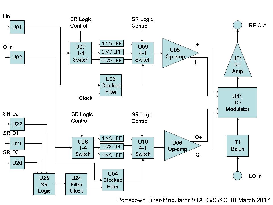
| + | |||
| + | *[[:Media:3 F-M Block.jpg| Block Diagram with IC Numbers]] | ||
| + | |||
| + | *[[:Media:RBTVMOD 30 SCH P1.pdf| Circuit schematic - part 1]] | ||
| + | |||
| + | *[[:Media:RBTVMOD 30 SCH P2.pdf| Circuit schematic - part 2]] | ||
| + | |||
| + | *[[:Media:RBTVMOD 30 SCH P3.pdf| Circuit schematic - part 3]] | ||
| + | |||
| + | These diagrams do not reflect the minor circuit changes for V1a, so read the information below. | ||
| + | |||
| + | ===Modifications to Improve the Transmitted Spectrum on Version 1 Boards=== | ||
| + | |||
| + | The Version 1 boards described above are OK to use on-air as any spurious emissions are about 50 dB below the main transmission, and the modulation "shoulders" will generally be in-band. However there are a few modifications that can be done to improve their output and reduce the level of the "shoulders" at SR1000 and above. The modifications also equalise the levels between low SRs (RB-TV) and higher SRs (1000 and above). | ||
| + | |||
| + | The following modifications improve the transmitted spectrum of the Version 1 PCBs, and bring them to Version 1A standard. | ||
| + | |||
| + | ===Spectrum plots of version 1a=== | ||
| + | |||
| + | Spectrum before modification - 1255MHz, 333ks, 5MHz/division | ||
| + | |||
| + | [[File:mod before.JPG|400px]] | ||
| + | |||
| + | |||
| + | Spectrum after modification - 1255MHz, 333ks, 5MHz/division | ||
| + | |||
| + | [[File:mod after.JPG|400px]] | ||
| + | |||
| + | |||
| + | Close-in spectrum after modification - 1255MHz, 333ks, 500KHz/division | ||
| + | |||
| + | |||
| + | [[File:333ks.JPG|400px]] | ||
| + | |||
| + | |||
| + | Spectrum after modification - 1255MHz, 1Ms, 5MHz/division | ||
| + | |||
| + | |||
| + | [[File:1ms.jpg|400px]] | ||
| + | |||
| + | |||
| + | Spectrum after modification - 1255MHz, 2Ms, 5MHz/division | ||
| + | |||
| + | |||
| + | [[File:2ms.jpg|400px]] | ||
| + | |||
| + | |||
| + | Spectrum after modification - 1255MHz, 4Ms, 5MHz/division | ||
| + | |||
| + | |||
| + | [[File:4ms.jpg|400px]] | ||
| + | |||
| + | ===Modification 1=== | ||
'''1. Reduce breakthrough (around 130 - 160 MHz) of the harmonics of the filter clock:''' | '''1. Reduce breakthrough (around 130 - 160 MHz) of the harmonics of the filter clock:''' | ||
Solder a 10n chip capacitor on the underside of the PCB between the +5v rail and ground near U10. The capacitor needs to be fitted between the thru-hole which feeds pin 5 of U10 and the adjacent square ground pad ON THE UNDERSIDE OF THE BOARD. The capacitor is visible in the upper left of this photo. | Solder a 10n chip capacitor on the underside of the PCB between the +5v rail and ground near U10. The capacitor needs to be fitted between the thru-hole which feeds pin 5 of U10 and the adjacent square ground pad ON THE UNDERSIDE OF THE BOARD. The capacitor is visible in the upper left of this photo. | ||
| + | |||
| + | [[File:Supply_Decoupling2.JPG|300px]] | ||
| + | ===Modification 2=== | ||
'''2. Reduce filter clock breakthrough on the I and Q signals:''' | '''2. Reduce filter clock breakthrough on the I and Q signals:''' | ||
| − | Solder 300 pf capacitors (chip or discrete) between the downstream ends of R15 and R16 and ground on the top side of the board. These capacitors form simple low pass filters with R15 and R16 to reduce clock breakthrough from the switched-capacitor filters. There is a convenient (square) ground pad just "north" of R15 and R16. A short wire link is required if using a chip capacitor adjacent to R16. Both are visible in this photo. | + | Solder 270 pf (or 300 pf) capacitors (chip or discrete) between the downstream ends of R15 and R16 and ground on the top side of the board. These capacitors form simple low pass filters with R15 and R16 to reduce clock breakthrough from the switched-capacitor filters. There is a convenient (square) ground pad just "north" of R15 and R16. A short wire link is required if using a chip capacitor adjacent to R16. Both are visible in this photo. |
| + | |||
| + | [[File:Clock_Capacitors2.JPG|600px]] | ||
| − | |||
| + | ===Modification 3=== | ||
'''3. Reduce the level of the drive to the IQ modulator at higher SRs (1000 KS and above).''' | '''3. Reduce the level of the drive to the IQ modulator at higher SRs (1000 KS and above).''' | ||
The original design slightly overdrove the IQ modulator at higher SRs, resulting in higher than necessary "shoulder" levels and differing power output depending on SR selection. This modification reduces the drive amplitude, but also affects the modulator balance and may require some "tweaking" of resistor values. | The original design slightly overdrove the IQ modulator at higher SRs, resulting in higher than necessary "shoulder" levels and differing power output depending on SR selection. This modification reduces the drive amplitude, but also affects the modulator balance and may require some "tweaking" of resistor values. | ||
| − | First, R03 and R04 (both 2400 ohms) need to be removed and replaced with 3300 ohm resistors. This reduces the I and Q levels to within the modulator specification but upsets the balance. Then R05 and R06 need changing from 4700 to | + | First, R03 and R04 (both 2400 ohms) need to be removed and replaced with 3300 ohm resistors. This reduces the I and Q levels to within the modulator specification but upsets the balance. Then R05 and R06 need changing from 4700 to 3900 ohms to restore the balance. You may find that a parallel resistor on R05 or R07 (for the I channel) or R06 or R08 (for the Q channel) may be required to align the quadrature balance point with that set for the lower (<1000K) SRs using RV1 and RV2. |
Latest revision as of 11:03, 22 March 2017
Board information - version 1
PCBs supplied before 28 February 2017 are Version 1 and the parts list and schematics are available for download:
These diagrams do not reflect the minor circuit changes for V1a, so read the information below.
Modifications to Improve the Transmitted Spectrum on Version 1 Boards
The Version 1 boards described above are OK to use on-air as any spurious emissions are about 50 dB below the main transmission, and the modulation "shoulders" will generally be in-band. However there are a few modifications that can be done to improve their output and reduce the level of the "shoulders" at SR1000 and above. The modifications also equalise the levels between low SRs (RB-TV) and higher SRs (1000 and above).
The following modifications improve the transmitted spectrum of the Version 1 PCBs, and bring them to Version 1A standard.
Spectrum plots of version 1a
Spectrum before modification - 1255MHz, 333ks, 5MHz/division

Spectrum after modification - 1255MHz, 333ks, 5MHz/division

Close-in spectrum after modification - 1255MHz, 333ks, 500KHz/division

Spectrum after modification - 1255MHz, 1Ms, 5MHz/division

Spectrum after modification - 1255MHz, 2Ms, 5MHz/division

Spectrum after modification - 1255MHz, 4Ms, 5MHz/division

Modification 1
1. Reduce breakthrough (around 130 - 160 MHz) of the harmonics of the filter clock:
Solder a 10n chip capacitor on the underside of the PCB between the +5v rail and ground near U10. The capacitor needs to be fitted between the thru-hole which feeds pin 5 of U10 and the adjacent square ground pad ON THE UNDERSIDE OF THE BOARD. The capacitor is visible in the upper left of this photo.

Modification 2
2. Reduce filter clock breakthrough on the I and Q signals:
Solder 270 pf (or 300 pf) capacitors (chip or discrete) between the downstream ends of R15 and R16 and ground on the top side of the board. These capacitors form simple low pass filters with R15 and R16 to reduce clock breakthrough from the switched-capacitor filters. There is a convenient (square) ground pad just "north" of R15 and R16. A short wire link is required if using a chip capacitor adjacent to R16. Both are visible in this photo.

Modification 3
3. Reduce the level of the drive to the IQ modulator at higher SRs (1000 KS and above).
The original design slightly overdrove the IQ modulator at higher SRs, resulting in higher than necessary "shoulder" levels and differing power output depending on SR selection. This modification reduces the drive amplitude, but also affects the modulator balance and may require some "tweaking" of resistor values.
First, R03 and R04 (both 2400 ohms) need to be removed and replaced with 3300 ohm resistors. This reduces the I and Q levels to within the modulator specification but upsets the balance. Then R05 and R06 need changing from 4700 to 3900 ohms to restore the balance. You may find that a parallel resistor on R05 or R07 (for the I channel) or R06 or R08 (for the Q channel) may be required to align the quadrature balance point with that set for the lower (<1000K) SRs using RV1 and RV2.