Difference between revisions of "Filter Modulator Version 1A Modifications"
(Created page with "The following modifications improve the transmitted spectrum of the Version 1 PCBs, and bring them to Version 1A standard: 1. Reduce breakthrough (around 130 - 160 MHz) of...") |
|||
| Line 1: | Line 1: | ||
The following modifications improve the transmitted spectrum of the Version 1 PCBs, and bring them to Version 1A standard: | The following modifications improve the transmitted spectrum of the Version 1 PCBs, and bring them to Version 1A standard: | ||
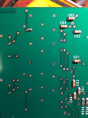
| − | 1. Reduce breakthrough (around 130 - 160 MHz) of the harmonics of the filter clock: Solder a 10n chip capacitor on the underside of the PCB between the +5v rail and ground near U10. The capacitor needs to be fitted between the thru-hole which feeds pin 5 of U10 and the adjacent square ground pad ON THE UNDERSIDE OF THE BOARD. | + | 1. Reduce breakthrough (around 130 - 160 MHz) of the harmonics of the filter clock: Solder a 10n chip capacitor on the underside of the PCB between the +5v rail and ground near U10. The capacitor needs to be fitted between the thru-hole which feeds pin 5 of U10 and the adjacent square ground pad ON THE UNDERSIDE OF THE BOARD. The capacitor is visible in the upper left of this photo. |
| + | [[File:Supply Decoupling.JPG|300px]] | ||
| + | |||
| + | 2. Reduce filter clock breakthrough on the I and Q signals: Solder 300 pf capacitors (chip or discrete) between the downstream ends of R15 and R16 and ground on the top side of the board. These capacitors form simple low pass filters with R15 and R16 to reduce clock breakthrough from the switched-capacitor filters. There is a convenient (square) ground pad just "north" of R15 and R16. A short wire link is required if using a chip capacitor adjacent to R16. Both are visible in this photo. | ||
| + | [[File:Clock Capacitors.JPG|300px]] | ||
Revision as of 15:42, 4 March 2017
The following modifications improve the transmitted spectrum of the Version 1 PCBs, and bring them to Version 1A standard:
1. Reduce breakthrough (around 130 - 160 MHz) of the harmonics of the filter clock: Solder a 10n chip capacitor on the underside of the PCB between the +5v rail and ground near U10. The capacitor needs to be fitted between the thru-hole which feeds pin 5 of U10 and the adjacent square ground pad ON THE UNDERSIDE OF THE BOARD. The capacitor is visible in the upper left of this photo.

2. Reduce filter clock breakthrough on the I and Q signals: Solder 300 pf capacitors (chip or discrete) between the downstream ends of R15 and R16 and ground on the top side of the board. These capacitors form simple low pass filters with R15 and R16 to reduce clock breakthrough from the switched-capacitor filters. There is a convenient (square) ground pad just "north" of R15 and R16. A short wire link is required if using a chip capacitor adjacent to R16. Both are visible in this photo.
