Difference between revisions of "CSI-2 to HDMI"
| Line 10: | Line 10: | ||
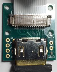
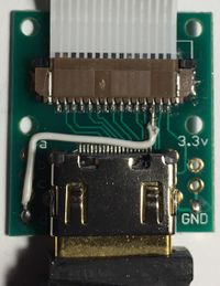
[[File:HDMI Stage 0.jpg|200px|left|thumb|Unmodified]][[File:HDMI Stage 1.jpg|200px|left|thumb|Modification 1]][[File:HDMI Stage 2.jpg|200px|left|thumb|Modification 2]] | [[File:HDMI Stage 0.jpg|200px|left|thumb|Unmodified]][[File:HDMI Stage 1.jpg|200px|left|thumb|Modification 1]][[File:HDMI Stage 2.jpg|200px|left|thumb|Modification 2]] | ||
| − | The HDMI pins are numbered from the left 19 to 1 on the right in the images above. The CSI-2 connector pins are numbered from 1 on the left to 15 on the right. The detailed pinout is below for reference. | + | The HDMI pins are numbered from 19 on the left 19 to 1 on the right in the images above. The CSI-2 connector pins are numbered from 1 on the left to 15 on the right. The detailed pinout is below for reference. |
Revision as of 12:30, 10 July 2017
It is possible to use an HDMI cable to extend the lead on the Pi Camera but some lower quality HDMI leads will not work without modifications to the Tindie connector cards https://www.tindie.com/products/freto/pi-camera-hdmi-cable-extension/. This is because some of them do not include the ground/shield connection for the 4 data pairs, and some do not include a wire for the Consumer Electronics Control (CEC) channel on pin 13.
There are 2 modifications required:
The first uses the overall cable screen to replace the non-existent data pair screens. To make this modification, simply use solder to bridge the 2 rectangular pads above to the "GND" caption on the right hand side of the HDMI socket. Thanks to Tindie and his blog http://petitstudio.blogspot.co.uk/2015/05/hdmi-cables-are-not-all-same.html for this modification.
The second modification uses one of the spare cores (labelled a, b, c and d) instead of the possibly non-existent Pin 13 CEC core. This modification requires a fine soldering iron and a magnifying glass to solder a wire between pin 13 on the CSI-2 flat cable connector (coincidentally connected to pin 13 on the HDMI connector) and the round pad labelled "d". Use a test meter to check that you have not created a solder bridge to pin 12 or pin 14 after making this modification. I chose the "d" pad because this is a data wire in the normal usage of HDMI.
The unmodified board, and the 2 modifications are shown below.
The HDMI pins are numbered from 19 on the left 19 to 1 on the right in the images above. The CSI-2 connector pins are numbered from 1 on the left to 15 on the right. The detailed pinout is below for reference.
| CSI-2 Pin | Name | Purpose | Tindie PCB | HDMI Pin | HDMI Name |
|---|---|---|---|---|---|
| 1 | Ground | Ground | Ground | 11 | Ground |
| 2 | CAM1_DN-0 | Data Lane 0 | 12 | TMDS Clk - | |
| 3 | CAM1_DP0 | Data Lane 0 | 10 | TMDS Clk + | |


