Difference between revisions of "PicoTuner Hardware"
(→Rev 3) |
(→Rev 3) |
||
| (12 intermediate revisions by 2 users not shown) | |||
| Line 32: | Line 32: | ||
The changes on the Rev 3 PCB are the addition of a power LED and all LEDs are now on the front panel. | The changes on the Rev 3 PCB are the addition of a power LED and all LEDs are now on the front panel. | ||
| − | * The Rev 3 parts list (BOM) is available here: [[:File: | + | * The Rev 3 parts list (BOM) is available here:[[:File:PicoTunerRev3_BOM.xlsx]] |
| − | * The Rev 3 schematic is available here [[:File: | + | * The Rev 3 schematic is available here [[:File:PicoTunerRev3.pdf]] |
| − | * The back panel design is here [[:File:BackPanel3.pdf]] | + | * The back panel design is here [[:File:BackPanel3.pdf]] This can be printed out (you will have to get the correct scaling on your printer) and tacked on to the Hammond case back panel and drilled. 3D STL[[:File:PicoBackPanelSTL.zip]] |
| − | The PCB | + | The blank PCB, available from the BATC shop looks like this: |
| − | [[File:Picotuner v3 board.jpg| | + | [[File:Picotuner v3 board.jpg|400px]] |
| + | |||
| + | and when built: | ||
[[File:PicoTunerRev3.jpg|600px]] | [[File:PicoTunerRev3.jpg|600px]] | ||
| Line 61: | Line 63: | ||
* Note, do not install the NIM or Pico until the PCB has been tested. | * Note, do not install the NIM or Pico until the PCB has been tested. | ||
| − | The LNB supply chip, if used, is the most challenging as it is an SMD device and has a pad on the base that needs to be soldered to the ground plane on the back side of the PCB for heat dissipation. So, start with this chip. First solder the chip pins to the PCB, taking care to get it in the correct place and flat against the board. When happy, turn over the board and with a large soldering iron, heat the pad and poke some solder through the small slot intended for this purpose. Do not use too much solder. It's not hard if you take care, but you need a decent thermal mass due to the copper ground plane. Use the correct tools, don't be tempted to try a small 25w iron that will take a long time slowly getting the joint up to solder melting point, as that will damage the chip. | + | The LNB supply chip, if used, is the most challenging as it is an SMD device and has a pad on the base that needs to be soldered to the ground plane on the back side of the PCB for heat dissipation. So, start with this chip. First solder the chip pins to the PCB, taking care to get it in the correct place and flat against the board. When happy, turn over the board and with a large soldering iron, heat the pad and poke some solder through the small slot intended for this purpose. Do not use too much solder. It's not hard if you take care, but you need a large iron to give a decent thermal mass due to the copper ground plane. Use the correct tools, don't be tempted to try a small 25w iron that will take a long time slowly getting the joint up to solder melting point, as that will damage the chip. |
I would then progress with regulators U4, U5 and U6, ensuring to get them in the right places, then the resistors, then D8, U1, D1, D2, the pin-headers JP1, 2 3 & 4, the DC socket and USB socket, the pin-sockets for the pico (not optional, trust me, you will need to remove it at some point), the ceramic capacitors the remaining diodes, C1, C5, the LEDs, the fuse holder, molex connectors and finally the electrolytics. | I would then progress with regulators U4, U5 and U6, ensuring to get them in the right places, then the resistors, then D8, U1, D1, D2, the pin-headers JP1, 2 3 & 4, the DC socket and USB socket, the pin-sockets for the pico (not optional, trust me, you will need to remove it at some point), the ceramic capacitors the remaining diodes, C1, C5, the LEDs, the fuse holder, molex connectors and finally the electrolytics. | ||
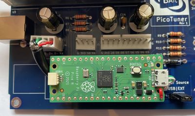
If you plan to use the type B USB port on the back panel, you will need to make up a patch lead to go from the Pico USB port to the white 4 pin Molex connector next to the USB socket. The best way is to cut up a good quality micro-USB cable. The pinout is marked on the silk screen. The "standard" is Red V+, Green D+, White D- and Black GND. You can also directly solder the USB lead to the Test Points under the USB socket on the Pico; the +V line can be routed through the adjacent hole abnd soldered to the top of Pin 40 as shown here. | If you plan to use the type B USB port on the back panel, you will need to make up a patch lead to go from the Pico USB port to the white 4 pin Molex connector next to the USB socket. The best way is to cut up a good quality micro-USB cable. The pinout is marked on the silk screen. The "standard" is Red V+, Green D+, White D- and Black GND. You can also directly solder the USB lead to the Test Points under the USB socket on the Pico; the +V line can be routed through the adjacent hole abnd soldered to the top of Pin 40 as shown here. | ||
| + | |||
| + | '''NOTE the correct way round to fit the Pico in the picture below''' | ||
[[File:USB Colours.jpg|400px]] | [[File:USB Colours.jpg|400px]] | ||
| Line 87: | Line 91: | ||
==Testing== | ==Testing== | ||
| − | The first thing to do is test the regulators, starting with U1. Select external | + | The first thing to do is test the regulators, starting with U1. |
| + | |||
| + | Select external power by shorting middle to EXT on JP4. Remember to fit the fuse and short JP1 to enable power in. Put 12v on the power input socket J1 and there should be 4.0-4.2V at TP3. There will be no supply to the rest of the regulators until JP4 is selected. | ||
However, as the regulators are not enabled there will be no output. To get an output it is necessary to temporarily short pins 1&2 on U4 or U6. This sets the enable pin high and the correct voltages should appear on TP4, TP5 and TP6. Once tested, remember to remove the short. | However, as the regulators are not enabled there will be no output. To get an output it is necessary to temporarily short pins 1&2 on U4 or U6. This sets the enable pin high and the correct voltages should appear on TP4, TP5 and TP6. Once tested, remember to remove the short. | ||
Latest revision as of 16:06, 6 January 2025
Mike G0MJW has designed a PCB that will host the Serit NIM and Pico board.
PCBs, BOM and schematic
PCBs will be made available in the shop from the beginning of April 2024.
https://batc.org.uk/shop/picotuner-blank-pcb/
Note:- The following pictures show the optional Wiznet version of the Pico with Integrated Ethernet Port. The basic Pico model is all you need for USB operation. The basic Pico (without wireless) comes in two versions, one with header pins (the Pico H) at about £5, and one without header pins (the Pico) at about £4.
Rev 1
Early PCBs from the BATC shop are at Rev 1.
- The parts list (BOM) is available here: File:PicoTunerADJBOM_updated.xlsx
- The schematic is available here File:PicoTuner-rev1.pdf
- A drawing for the back panel is here File:BackPanel.pdf
- If you want to 3D print a template, this may help File:3DPicoBackPanelPad.zip
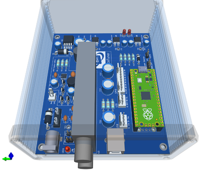
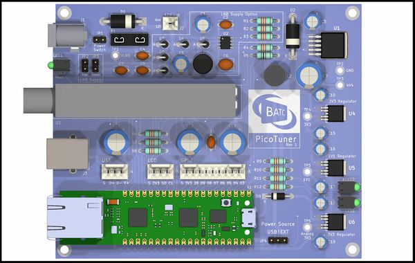
It should look a bit like this (Excepting R4 value)
Rev 3
The changes on the Rev 3 PCB are the addition of a power LED and all LEDs are now on the front panel.
- The Rev 3 parts list (BOM) is available here:File:PicoTunerRev3_BOM.xlsx
- The Rev 3 schematic is available here File:PicoTunerRev3.pdf
- The back panel design is here File:BackPanel3.pdf This can be printed out (you will have to get the correct scaling on your printer) and tacked on to the Hammond case back panel and drilled. 3D STLFile:PicoBackPanelSTL.zip
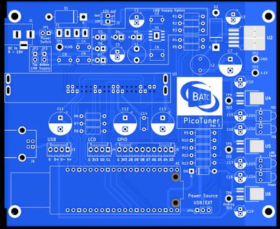
The blank PCB, available from the BATC shop looks like this:
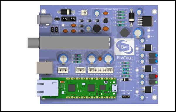
and when built:
Parts Availability
The continued availability of specified components is an ongoing problem for designs such as this.
The 3v3 regulator TPS78533 can be substituted with the onsemi NCV5661DT33RKG, available from DigiKey with part number NCV5661DT33RKGOSCT-ND.
Build instructions
Construction is straight forward and best done according to the height of the components being fitted.
Important notes
- It is recommend that the Rpi Pico is placed in a socket and not soldered directly.
- Note the Pico orientation - the USB socket must point away from the edge of the PCB. The pictures above show the optional Wiznet version of the Pico with Integrated Ethernet Port. A standard Raspberry Pi Pico (non-wifi) is all that is required for a USB connected PicoTuner.
- Note, do not install the NIM or Pico until the PCB has been tested.
The LNB supply chip, if used, is the most challenging as it is an SMD device and has a pad on the base that needs to be soldered to the ground plane on the back side of the PCB for heat dissipation. So, start with this chip. First solder the chip pins to the PCB, taking care to get it in the correct place and flat against the board. When happy, turn over the board and with a large soldering iron, heat the pad and poke some solder through the small slot intended for this purpose. Do not use too much solder. It's not hard if you take care, but you need a large iron to give a decent thermal mass due to the copper ground plane. Use the correct tools, don't be tempted to try a small 25w iron that will take a long time slowly getting the joint up to solder melting point, as that will damage the chip.
I would then progress with regulators U4, U5 and U6, ensuring to get them in the right places, then the resistors, then D8, U1, D1, D2, the pin-headers JP1, 2 3 & 4, the DC socket and USB socket, the pin-sockets for the pico (not optional, trust me, you will need to remove it at some point), the ceramic capacitors the remaining diodes, C1, C5, the LEDs, the fuse holder, molex connectors and finally the electrolytics.
If you plan to use the type B USB port on the back panel, you will need to make up a patch lead to go from the Pico USB port to the white 4 pin Molex connector next to the USB socket. The best way is to cut up a good quality micro-USB cable. The pinout is marked on the silk screen. The "standard" is Red V+, Green D+, White D- and Black GND. You can also directly solder the USB lead to the Test Points under the USB socket on the Pico; the +V line can be routed through the adjacent hole abnd soldered to the top of Pin 40 as shown here.
NOTE the correct way round to fit the Pico in the picture below
| Signal | Colour | Pico TestPoint |
|---|---|---|
| Gnd | Black | TP1 |
| Data+ | Green | TP3 |
| Data- | White | TP2 |
| V+ | Red | Pin 40 |
Approximate build time is 2 hours.
Testing
The first thing to do is test the regulators, starting with U1.
Select external power by shorting middle to EXT on JP4. Remember to fit the fuse and short JP1 to enable power in. Put 12v on the power input socket J1 and there should be 4.0-4.2V at TP3. There will be no supply to the rest of the regulators until JP4 is selected.
However, as the regulators are not enabled there will be no output. To get an output it is necessary to temporarily short pins 1&2 on U4 or U6. This sets the enable pin high and the correct voltages should appear on TP4, TP5 and TP6. Once tested, remember to remove the short.
If all is OK, fit the Pico and move the supply JP4 to USB. Connect the Pico to a USB port and repeat the testing for TP4, TP5 and TP6. You may also want to install the firmware - see below.
That completes the testing, but it won't work yet until the NIM is fitted, so do that next. Be careful not to bend any pins on installing it, it should be an easy fit, if it isn't something is wrong. Make sure it is straight and properly seated, then solder the tabs. Only solder the pins after checking everything is correctly placed.
Programming the Pico
This can be done either before or after the Pico has been fitted to the PCB, it makes no difference. Updating to a new firmware version is done the same way.
1. Locate the latest compiled firmware file 'PicoTuner_vxxx.uf2' which will be found here https://github.com/g4eml/PicoTuner/releases and save it to your desktop.
2. Hold down the BOOTSEL button on the Pico while connecting it to your PC using its micro USB port. The Pico should appear as a USB disk drive on your PC.
3. Copy the .uf2 file onto the USB drive. The Pico will recognise the file and immediately update its firmware, reboot and the PC should recognise a new USB device.
