Difference between revisions of "PTT and band switching"
| Line 92: | Line 92: | ||
| 2 || - || - || 5v || || | | 2 || - || - || 5v || || | ||
|- | |- | ||
| − | | 3 || 2 || 8 || | + | | 3 || 2 || 8 || SDA 1 || || |
|- | |- | ||
| 4 || - || - || 5v || || | | 4 || - || - || 5v || || | ||
|- | |- | ||
| − | | 5 || 3 || 9 || | + | | 5 || 3 || 9 || SCL 1 || || |
|- | |- | ||
| 6 || - || - || 0v || || | | 6 || - || - || 0v || || | ||
|- | |- | ||
| − | | 7 || | + | | 7 || 4 || 7 || GPIO 7 || || (was DigiThin) |
|- | |- | ||
| − | | 8 || | + | | 8 || 14 || 15 || TxD || || (was DigiThin) |
|- | |- | ||
| 9 || - || - || 0v || || | | 9 || - || - || 0v || || | ||
|- | |- | ||
| − | | 10 || | + | | 10 || 15 || 16 || RxD || || (was DigiThin) |
|- | |- | ||
| − | | 11 || | + | | 11 || 17 || 0 || GPIO 0 || LCD Display || - |
|- | |- | ||
| − | | 12 || | + | | 12 || 18 || 1 || GPIO 1 || || (was DigiThin) |
|- | |- | ||
| − | | 13 || | + | | 13 || 27 || 2 || GPIO 2 || Shutdown LED || |
|- | |- | ||
| 14 || - || - || 0v || || | | 14 || - || - || 0v || || | ||
|- | |- | ||
| − | | 15 || | + | | 15 || 22 || 3 || GPIO 3 || Shutdown Button || |
|- | |- | ||
| − | | 16 || | + | | 16 || 23 || 4 || GPIO 4 || LCD Display || - |
|- | |- | ||
| − | | 17 || | + | | 17 || - || - || 3.3v || || |
|- | |- | ||
| − | | 18 || | + | | 18 || 24 || 5 || GPIO 5 || LCD Display || - |
|- | |- | ||
| − | | 19 || | + | | 19 || 10 || 12 || MOSI || LCD Display || - |
|- | |- | ||
| 20 || - || - || 0v || || | | 20 || - || - || 0v || || | ||
|- | |- | ||
| − | | 21 || Example || Example || Example || | + | | 21 || Example || Example || Example || LCD Display || - |
|- | |- | ||
| 22 || Example || Example || Example || Example || Example | | 22 || Example || Example || Example || Example || Example | ||
Revision as of 16:22, 13 January 2018
In order to make the Portsdown transmitter integrated with transmit and receive systems, Pin 40 of the GPIO goes high when transmit is selected and the signals on pins 28 and 35 can be used for band switching.
Band outputs
These outputs are used to switch the LO filter and can be used to switch external filter and amplifiers.
| Frequency Mhz | ATV Band | Pin 28 | Pin 35 |
|---|---|---|---|
| < 100 MHz | 71 MHz | Lo | Lo |
| 100 - 250 MHz | 146 MHz | Lo | Hi |
| 250 - 950 MHz | 437 MHz | Hi | Lo |
| 950 - 4400 MHz | 23cms | Hi | Hi |
Care must be taken to properly buffer these 3.3v signals from relay transients.
GPIO band decoder
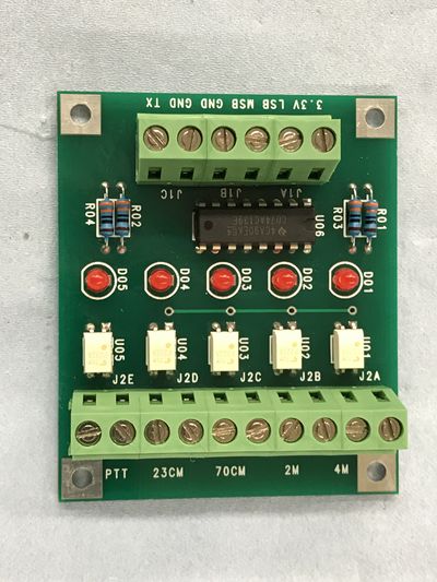
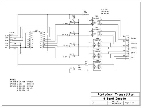
As we only have 2 GPIO pins to provide 4 outputs, these outputs need to be decoded to provide an output for each band.
The Portsdown team have designed a simple board which can be either constructed on 0.1” perforated board (veroboard) or on a PCB - this can be home etched using the details below or blank PCBs are available in the BATC shop.
File:DECODE 4 Band instructions (2).pdf
File:Decode 4 Band Schematic.pdf
File:Decode 4 Band Perf Bd wiring.pdf
File:DECODE 4 Band Mirrored w SS.pdf
File:DECODE 4 Band Mirrored.pdf
File:DECODE 4 Band PCB Layout w SS.pdf
PTT steering
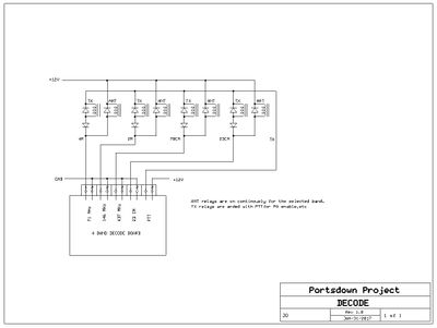
These band outputs can then used to "steer" the PTT line to the correct Power Amplifier using this simple relay and diode circuit - no PCB needed :-)
Tx Rx sequencer
We also recommend the use of a Tx / Rx sequencer to ensure your mast head relay has changed over and your expensive pre-amp is de-powered before you start transmitting. The sequence is as follows:
To go to Tx:
1) Turn off receiver pre-amp
2) Switch ant c/o relay to transmit
3) Apply power to PA
To go to rx
a) Turn off Tx
b) Switch ant c/o relay to receive
c) Apply power to pre-amp.
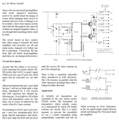
Many circuits and pre-built designs are available including this simple single chip design by Ian Waters G3KKD published in CQ-TV 125.
David M0YDH shows Ian's design in operation:- G8ADE RELAY SEQUENCER VIDEO and an updated version with extra relay for Portsdown PTT band switching.
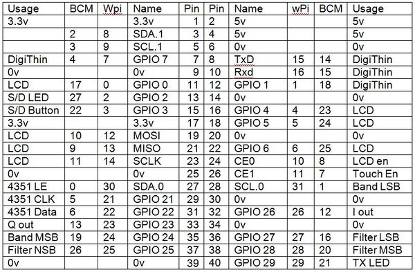
Summary of GPIO connections
As the Portsdown project has expanded in scope, so has demand for the GPIO connections on the RPi. Here is the latest list as of January 2018:
| Pin No | BCM No | Wiring Pi | RPi Name | Primary Use | Secondary Use |
|---|---|---|---|---|---|
| 1 | - | - | 3.3v | ||
| 2 | - | - | 5v | ||
| 3 | 2 | 8 | SDA 1 | ||
| 4 | - | - | 5v | ||
| 5 | 3 | 9 | SCL 1 | ||
| 6 | - | - | 0v | ||
| 7 | 4 | 7 | GPIO 7 | (was DigiThin) | |
| 8 | 14 | 15 | TxD | (was DigiThin) | |
| 9 | - | - | 0v | ||
| 10 | 15 | 16 | RxD | (was DigiThin) | |
| 11 | 17 | 0 | GPIO 0 | LCD Display | - |
| 12 | 18 | 1 | GPIO 1 | (was DigiThin) | |
| 13 | 27 | 2 | GPIO 2 | Shutdown LED | |
| 14 | - | - | 0v | ||
| 15 | 22 | 3 | GPIO 3 | Shutdown Button | |
| 16 | 23 | 4 | GPIO 4 | LCD Display | - |
| 17 | - | - | 3.3v | ||
| 18 | 24 | 5 | GPIO 5 | LCD Display | - |
| 19 | 10 | 12 | MOSI | LCD Display | - |
| 20 | - | - | 0v | ||
| 21 | Example | Example | Example | LCD Display | - |
| 22 | Example | Example | Example | Example | Example |
| 23 | Example | Example | Example | Example | Example |
| 24 | Example | Example | Example | Example | Example |
| 25 | Example | Example | Example | Example | Example |
| 26 | Example | Example | Example | Example | Example |
| 27 | Example | Example | Example | Example | Example |
| 28 | Example | Example | Example | Example | Example |
| 29 | Example | Example | Example | Example | Example |
| 30 | - | - | 0v | ||
| 31 | Example | Example | Example | Example | Example |
| 32 | Example | Example | Example | Example | Example |
| 33 | Example | Example | Example | Example | Example |
| 34 | - | - | 0v | ||
| 35 | Example | Example | Example | Example | Example |
| 36 | Example | Example | Example | Example | Example |
| 37 | Example | Example | Example | Example | Example |
| 38 | Example | Example | Example | Example | Example |
| 39 | - | - | 0v | ||
| 40 | 21 | 29 | GPIO 29 | TX LED and PTT | - |
The BCM numbers in this table correspond to the connector labelling on the Willow Electronics GPIO breakout board. Two of the connections are not broken out and need to be directly connected to the GPIO pins. More details to follow.
