Difference between revisions of "Assembling Portsdown"
| Line 5: | Line 5: | ||
==Mechanical Design== | ==Mechanical Design== | ||
| − | First of all, decide on your mechanical design. You are going to need to have the RPi firmly mounted, with the Micro-SD card slot accessible (to change the card if required) and the power, network and USB connectors available. Then you will need to stack a GPIO extender | + | First of all, decide on your mechanical design. You are going to need to have the RPi firmly mounted, with the Micro-SD card slot accessible (to change the card if required) and the power, network and USB connectors available. Then you will need to stack a GPIO extender on top of the RPi. |
| − | You will then need to consider mounting the ADF4351 Synthesizer, any LO filters and then the Filter/modulator board. Other things to think about might be a 5V power supply, a relay/PTT switching board and any dongles (EasyCap, Sound or RTL-SDR). The block diagram of what you are trying to achieve is below. Note that you will need an additional filter between the synthesizer and the filter/modulator board for 437 MHz and 146 MHz. It is not required for 1255 MHz, and the unit will work on the other bands for testing without it. | + | The most difficult part will be to mount the Touchscreen display. It can either be stacked on top of the RPi, or you can connect it by a short multiway lead and mount it on the front panel of your housing. |
| + | |||
| + | You will then need to consider mounting the ADF4351 Synthesizer, any LO filters and then the Filter/modulator board. Other things to think about might be a 5V power supply, a relay/PTT switching board and any dongles (EasyCap, Sound or RTL-SDR). | ||
| + | |||
| + | The block diagram of what you are trying to achieve is below. Note that you will need an additional filter between the synthesizer and the filter/modulator board for 437 MHz and 146 MHz. It is not required for 1255 MHz, and the unit will work on the other bands for testing without it. | ||
[[File:1-1 Block Diagram.jpg|800px]] | [[File:1-1 Block Diagram.jpg|800px]] | ||
Revision as of 13:36, 26 January 2017
This section will describe in detail how to assemble your Portsdown transmitter - to begin, you need to have bought or built all the components listed in the hardware description.
You can run the Portsdown as an experiment in "Ugly Mode", currently labelled in the Menu as QPSKRF. That does not require you to wire anything together. This page describes how to build the complete transmitter assembly.
Mechanical Design
First of all, decide on your mechanical design. You are going to need to have the RPi firmly mounted, with the Micro-SD card slot accessible (to change the card if required) and the power, network and USB connectors available. Then you will need to stack a GPIO extender on top of the RPi.
The most difficult part will be to mount the Touchscreen display. It can either be stacked on top of the RPi, or you can connect it by a short multiway lead and mount it on the front panel of your housing.
You will then need to consider mounting the ADF4351 Synthesizer, any LO filters and then the Filter/modulator board. Other things to think about might be a 5V power supply, a relay/PTT switching board and any dongles (EasyCap, Sound or RTL-SDR).
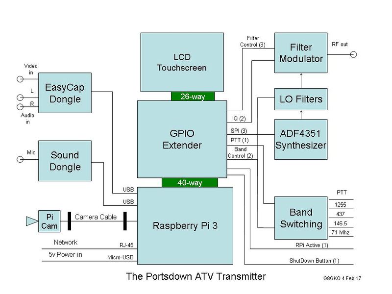
The block diagram of what you are trying to achieve is below. Note that you will need an additional filter between the synthesizer and the filter/modulator board for 437 MHz and 146 MHz. It is not required for 1255 MHz, and the unit will work on the other bands for testing without it.
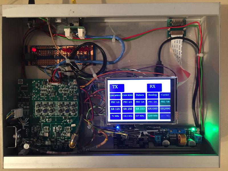
An example layout is here
Signal Wiring
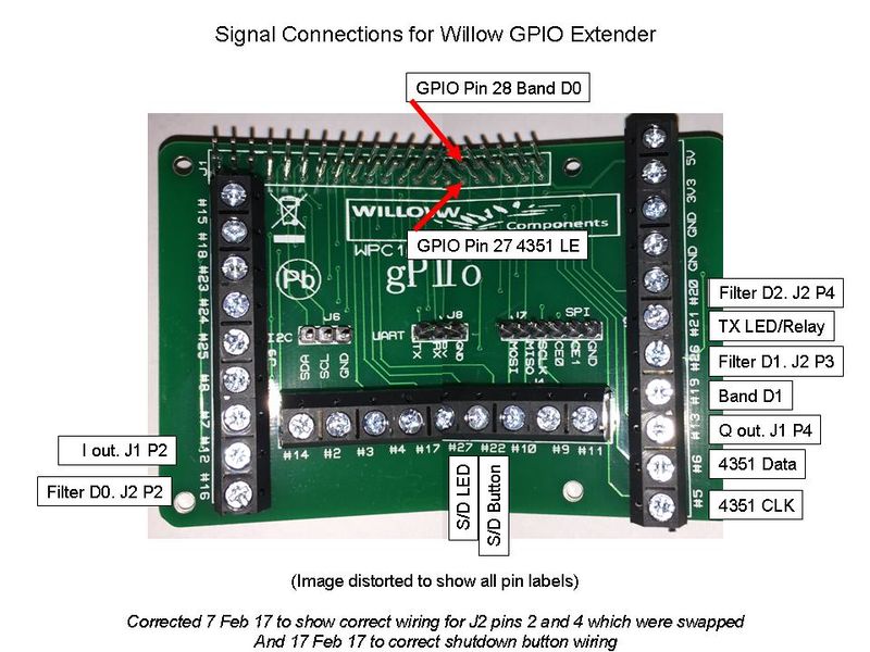
Once you have the mechanical design, you can start wiring up. The signal wiring from the Willow Components GPIO Extender board is complex and illustrated below. The nnumbers on the Willow Board refer to the BCM (Broadcomm) numbers in the table below.
Note that 2 of the signals are not broken out to the screw connectors on the Willow board, and so you will need to solder thin wires to extended GPIO pins 27 and 28. Using thin wires it is possible to do this and still mount the display directly above the board.
The design team realise that this board is not ideal, and a custom GPIO break-out board is being developed for sale in the BATC Shop.
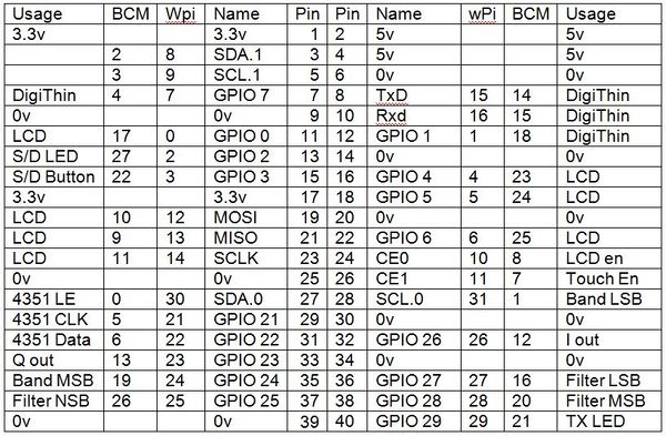
The full wiring listing for the RPi GPIO is here
RF Wiring
Use short flexible SMA cables to connect the ADF4351 (through filters if necessary) to the filter/modulator board. Use another cable to take the output to a panel connector or subsequent filters and power amplifiers.
You may also want to extend the input of any RTL-SDR to be accessible from a panel connector.
Power Wiring
You should power the RPi through the Micro-USB power connector to take advantage of the input protection provided. Use a very short USB cable to your power supply as most of these cables are of very poor quality and cause significant voltage drop. If you see a "Lightning Flash" symbol at the top right of your LCD display it means that the voltage at the RPi is too low. You can measure the voltage between the GPIO connector pins 4 and 6.
The ADF4351 will operate from the same 5V supply as the RPi. It has an on-board regulator to 3.3V, and digital noise on the power supply has not been observed to cause any problems.
The filter/modulator board needs a clean 5V at 250 mA and the on-board linear regulator supplies this, but can get warm at higher input voltages. It needs at least 9V to operate properly.
An eBay buck regulator capable of supplying at least 1A continuous at 5V is recommended to power the RPi and ADF4351.
Network and USB Wiring
Consider bringing the network connector and one of the USB connectors out to the panel for easy access and mechanical stability.
Camera Wiring
The Pi Camera has a short ribbon cable supplied, which is good if you want to mount it in the same box as the RPi, but if you want to have the camera separate, you will need to arrange an extension. The HDMI physical interface is good for this, and kits can be purchased for direct connection. Note that the Pi Camera signals are NOT HDMI, they are CSI-2 format signals - totally different.


